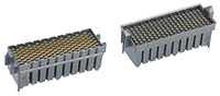
Ideal for space-constrained designs with a limited PCB real estate, the modular NeoScale mezzanine system from Molex provides a durable and easily customizable design tool for high-density system applications. Each NeoScale triad wafer is an independent element in the housing and can be customized to a design layout. With four triad wafer configurations, customers can mix-and-match components to build a mezzanine solution to meet their requirements for signals supporting high-speed differential pairs (85 ohm and 100 ohm), high-speed single-ended transmissions, low-speed single-ended signals, and power contacts.
Video: NeoScale High-Speed Mezzanine System
| Features |
|
|
- Patent-pending modular triad wafer design with four triad configurations and high-speed differential pairs (in both 85 ohm and 100 ohm impedance), high-speed single-ended traces, low-speed single-ended lines, and power contacts provides a customized system for design flexibility
- Housing design based on honeycomb construction isolates each differential pair for optimal performance and customization
- High-speed triad wafers comprise three-pins per differential pair (two signal pins and one shielded ground pin) providing stand-alone 28+ Gbps fully shielded differential pairs with dedicated grounds
- Connectors feature 246 circuits with a density of 82 differential pairs per square inch offers ultra-high-density signal solution with optimal signal integrity performance
- Mirror-image triad layout enables the PCB routing in one or two layers for four- and six-row housings respectively providing ease in PCB routing and lowers overall system costs by decreasing the number of PCB layers required for signal routing
|
|
- Tombstone structures incorporated within the receptacle housing prevents terminal damage by protecting the mating contact interface
- Innovative PCB connection using patented Solder-Charge Technology; proven surface mount technology (SMT) attach method for highly reliable and robust solder joints
- Available in 12 mm to 42 mm stack heights, circuit sizes of 8 to 300 triad wafers in 2-, 4-, 6-, 8-, and 10-rows and 85 ohm or 100 ohm impedance provides design flexibility to address engineering constraints in system envelopes
- Reliable mating interface with 2 mm wipe gives sufficient conductive wipe for clean signal transmission and enhanced performance
- Durable housing material provides a robust system with mechanical stability
|
| Specifications |
|
|
- Reference Information
- Packaging: tray
- Mates with NeoScale vertical plug (series 170807) or with NeoScale vertical receptacle (series 170814)
- Designed in millimeters
- RoHS: yes
- Halogen-free: yes
- Electrical
- Voltage (max): 30 VAC(rms) max
- Current (max): 1 A
- Contact resistance: 30 mΩ max
- Dielectric withstanding voltage: 200 VAC(rms)
- Insulation resistance: 1,000 MΩ mini
|
|
- Mechanical
- Contact retention to housing: 1 N
- Mating force: 0.75 N maximum
- Unmating force: 0.25 N minimum
- Durability (minimum): 100 cycles
- Physical
- Housing: high-temperature LCP
- Contact: copper (Cu)
- Plating: contact area – 30 μ" gold (Au); solder tail area – 15 μ" gold (Au); underplating – 45 μ" nickel (Ni)
- Operating temperature: -55°C to 85°C
|